Showing posts with label electronic engineering. Show all posts

Hat for Raspberry Pi to monitor environmental conditions (my sandbox for learning modern DevOps tools).

It’s 2024, and technologies from web development have made their way into the embedded world too-things like containerization, automated deployment, and more. This project is a small hat for the Raspberry Pi that gathers measurements for temperature, humidity, and air pressure. I created it as a learning tool to explore these concepts while using Docker, Ansible, and Grafana.

The picture below shows the hat. I thought it was so simple that I wouldn't make any mistakes during assembly, but, as usual, I did. The PCB turned out to be too long and collides with the USB port of the Raspberry Pi. That’s why I had to connect it using jumper wires. It works, but it doesn’t look very cool.

I didn’t choose these sensors for any particular reason—they were just parts I had on hand from the good pre-COVID times when software components and sensors were still cheap :)

The circuit is shown below. It consists of two sensors that communicate via I2C with the Raspberry Pi, along with a small LCD that also uses I2C. The LCD displays the measurement data as well.

Some people say that if your Raspberry Pi starts slowing down, it’s a sign that the SD card is about to fail, so it’s time to back up. I noticed mine was slowing down, checked the kernel logs, and everything looked fine, so I figured I was safe. The next day, the SD card was dead. So yeah, it’s definitely a good idea to back up in such cases.

This happened before I got into Docker and all the containerization stuff, so I was just developing scripts directly on the Raspberry Pi—and I think I lost them. It’s funny how I started this project to learn about containerization as a reliable way to deploy code, and I kicked things off with such a fail!

From the software point of view, the project will consist of three components:

  • Python software for gathering data from the sensors
  • InfluxDB for storing the measurements
  • Grafana for data analysis and presentation

I think each of these components will have its own Docker container. In addition, I’ve already created a Docker container for cross-compilation (since my PC has x86 architecture and the Raspberry Pi uses ARM architecture). It was quite a struggle to get that working. I plan to automate the installation using Ansible.

If you’re interested in the details, the full project is available on GitHub and Hackaday. Feel free to explore, make your own modifications, and maybe even improve on what I’ve done. And if you find it useful, don’t forget to share it!

Hardware Data Logger based on STM32 Nucleo and ESP Module

It's been a while since I last posted here, but here I am with something new. This project started when I was cleaning up the repo for a semiconductor radioactivity detector. For that project, I made a small shield for the STM32 Nucleo that included a button and a display.

It was used to present measurements in real time on the display and send them to a Raspberry Pi for further processing. I thought this could be turned into a separate project and reused, and I'll be presenting the results of that in this post. Here is the link to the GitHub of this new project that I describe in this post.

I started working on a new version and came up with these specs:

  • Keep the STM32 Nucleo as the main microcontroller
  • Add an ESP module for remotely uploading data to a Raspberry Pi or any other device
  • Use a much larger color display
  • Include four buttons for interacting with the device
  • Add 4 BNC connectors for gathering data from other devices
  • Include an SD card slot for local data storage
  • It also has a light sensor to dim the display at night.

The picture below shows the version that includes these specifications. Fun fact is that I traveled with this device in my carry-on luggage and was worried there might be issues at security, since it kind of looks like a movie bomb, but everything went fine.

Based on the that version, I created a dedicated PCB. I thought assembling the PCB would be pretty simple, but unfortunately, I forgot to buy all the components, which made it much harder than I expected. In this version, I used SMD female pins to connect to the Nucleo board. However, since I didn't have them on hand, I used THT pins instead. The footprint was different, and I didn’t solder them well, which put a lot of stress on the Nucleo board when connecting the shield.

It kept breaking repeatedly, and I didn’t expect such a small issue to cause so many problems. The LCD no longer works—probably something broke again—but the rest of the setup is functioning. In this version, the STM and ESP communicate with each other, but only in a limited way.

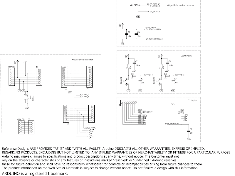
The device was designed in KiCad, and the circuit is shown below.

The firmware was developed using STM32CubeMX (for peripheral configuration), CMake, and C++17. I didn’t use anything from the standard library or dynamic memory allocation.

I’ve also included several tools for checking code quality: unit tests (Google Test, Google Mock), code coverage, static code analysis (cppcheck), and even dynamic code quality checks (which don’t make much sense in my case since I explicitly avoid using dynamic memory allocation, but I wasn’t thinking about that at the time). There are also Doxygen comments and coverage reports to flag any missing documentation.

I used ChatGPT (paid version) for most of this configuration. It’s amazing but can also help you quickly generate garbage. It speeds things up when you're headed in the right direction, but if you're doing something silly, it will just help you do it faster. You can check out how the CMake files are written in this project to get an idea of what I mean.

The current version is not finished, and I think I’ll abandon it in favor of a new version. I plan to drop the Nucleo board and place the STM chip directly on the PCB. This will solve the connector issues and make the device smaller and cheaper.

Another idea I have is to use some slots (similar to the ones used for connecting RAM to a PC motherboard, though I haven’t researched the names or footprints yet). This way, I could have one main PCB with the STM, ESP, display, etc., and use detachable boards for acquisition modules.

This is just the beginning, and there’s plenty of room for improvement. If you're curious to see where it goes, don't forget to watch or star the project on GitHub!

Camera nuclear-radiation sensor: part I

In previous posts I've described a radioactivity detector based on a photodiodes. Image sensors in cameras use photoelements too, so I think that they could be also used to detect radioactivity. At this moment i didn't success in this , nevertheless I will describe here my attempts.

I'm using RaspbberyPI, to get data from the sensor, camera is some low-budget/quality clone designed for RaspberryPI. I have removed optics, and covered whole camera in black tape to block any light coming to the sensor. It's visible on the picture below.

To handle the camera on the software side, I'm using Python script (with PiCamera library). In infinitive loop it takes a photo and calculate sum of pixels value and then sums values of each RGB channel. This value with timestamp is put to CSV file that is later parsed to diagrams using R script.

Without any sample, internal noise of the sensor (and maybe background radiation) should give after some time (e.g. after a couple of hours) a Gaussian curve on the histogram. After putting measured sample to the sensor and waiting similar period, a new Gaussian curve would appear, so that the histogram would have to visible peaks. That was my assumption, hit would prove that the sensor works, however as visible below it doesn't - there is only one peek.

I will try to better isolate the sensor also from electromagnetic noise or maybe buy a new camera (less noisy). Other than that I don't have ideas to make it works.

Semiconductor nuclear-radiation sensor: part III

In this post I will present a new hardware version of my sensor, older versions are described in part I and part II. In comparison to the previous one, sensitivity is roughly x10 more sensitive.

In previous version, tin foil window for photodiodes was very close to the BNC sockets and because enclosure was small, it was hard to place a sample close enough. Not it's better, however, if I would choosing again, I would use metal enclosure similar to those used in PC oscilloscopes and put BNCs on front panel, power socket on rear panel and tin foil window on top. This would allow me to easier access for debugging- now I have to desolder sockets to get to photodiodes or to bottom side of PCB (fortunately this side is empty).

Bellow you can see the diagram (click on it to enlarge), what has changed in comparison to previous version:

  • One additional photodiode (previous version has only two of them) to increase sensitivity, also the window in enclosure is much bigger
  • x10 bigger resistance of the feedback loop resistor in first stage amplifier, I tried bigger, but then osculations started
  • Bias for photodiodes using 12V batteries, I could increase it, but didn't have enough space in this enclosure
  • Buffer op-amp at the analog output
  • Digital output.

Additional changes not shown on diagram:

  • U1 is OPA657U
  • U2 is OPA656U
  • R4 is 1G
  • As close as possible to input power socket are placed in paraller 1n/16V and 100n/16V, without them the device started to oscillate randomly.
  • A Schottky diode is connected in series after mentioned above extra capacitors to reduce risk of damaging the device when power supply is connected incorrectly. I don't know if it will help enough but I have already broke one PCB of this device this way, so now it's there.

Digital output is 12V in high state, 0V in low state, this is not very useful for 3V3 logic microcontroller that I'm using for data acquisition, so I made a simple converter using additional PCB.

Here it is visible soldered. I like in those SMA Female sockets that they can be soldered to the edge of the PCB (as visible below) and this is still quite mechanically stable, but doesn't require to drill holes as in regular mounting way.

All materials (including software part presented in previous post) for this hardware revision can be downloaded from project's repository.

Semiconductor nuclear-radiation sensor: part II

There are many ways to measure radioactivity level, semiconductor detectors sense interactions between ionizing radiation and p-n junction. Because in hobbyist area most popular are Geiger-Muller based detectors (in short: not a semiconductor but lamp based devices), I think it's a cool idea to take a look at this approach.

In this post I will present such home-made sensor and a set of software to parse collected results.

Picture below presents circuit of the sensor that I made, it consist of a photodiode that acts as a sensor, transimpedance amplifier and "regular" amplifier. I've selected op-amps that has little input noise.

Changes that I made during testing the device, that are not presented on the diagram:

  • D1 is BPW34
  • U1 is OPA657U
  • U2 is OPA656U
  • 2p capacitor is connected in parallel with R6
  • 820k resistor is connected between U2 out and BNC socket.

Below is visible sensor in enclosure and without it. Because the device is sensitive for background EMI and light noise, a metal housing is needed. To increase exposure of the sensor to the radiation, where it is, in the housing, a hole is made and just a tiny adhesive metal tape is covering it.

Collecting data from measurements devices using USBTMC, SCPI, Python and R

High end test gear allows two-way communication with PC to set measurement parameters and to send the measured data to PC for further analyze. On PC side there are applications for this (LabView, BenchVue), but they are expensive. One option is to make own program/script that will communicate with the device and parse/present measured data - this approach I will present it in this post. The tool I'm using it with is 34460A(digital multimeter).

Below is an example of the measurement graph made using this home-made software.

The module of communication with the device I made in Python, it stores data to .csv file, that is later parsed by a script in R and the output graph is stored as .png image. The R part could ass well do some numeric stuff and print it on STDOUT, but for me that was not the case.

Initially all was in Python, but I didn't like Python's graphs, they weren't visually nice.

Python part when started will save measurements to the .csv file constantly, at any time, user can run R script to create new graph.

Installation steps

Assuming device driver correctly enumerate in the Device Manager (if not one needs to install its drivers first).

  • Install Python and R, add them to Path (environment variable).
  • In R, install following packages: latticeExtra, gridExtra, grid.
  • In Python install following packages: usbtmc, pyusb.
  • On Windows, download libusb-win32 and follow README steps to bind it to the device. In addition it didn't work for me if I didn't run the tool as an Administrator. If everything went ok, device will be visible in Device Manager in branch named libusb-win32 devices.
  • Download Python/R scripts, they are available via my IonizationChamber repository.
  • In main.py, replace idDMM with id of the device.

For usbtmc, I got the same problem as described here, fortunately the fix presented in that thread fixed it, so please check it if you have some weird stacktrace errors in Python.

Usage

I made those scripts for my personal use, so they may be a bit awkward to work with, but once the setup is done, everything should work fine.

  • Set meassurement type and range on your device (this could be also done via python script)
  • Start python script
  • Run R script, it will create results.png file with graphs.

That's all.

Negative resistance oscillators

Normally -according to the Ohm's law- when the applied voltage is increasing, the current is increasing too, however some components can break this law. When the voltage increases, current decreases. This is called negative resistance.

One of the most know element that exhibits this behavior is a tunnel diode. Once very promising, today it isn't widely used in popular designs and occupies a niche in microwave applications. It's a bit challenging to get one, fortunately simple circuits that have negative resistance feature can be build from popular discrete elements. One of them I will present today.

The circuit is so called "negistor" - a regular npn transistor connected in a way that the base is not connected at all, and collector-emiter junction is polarized in reverse direction. The generator that uses negative resistance is presented below, and consists of R1, C1 and T1, the voltage when it works is between 9-12V, R2, C2 are used to block DC voltage, D1 is used to indicate if the generator works. T1 works as the negistor.

It's worth noticing that the tunnel diode works due to a quantum effect called quantum tunelling, I'm not exactly sure if the negistor works also due to it.

Below you can see the voltage on the TP1 (test point), on the first image the scope was is in DC coupled mode, on the second in AC coupled mode.

Other configurations od the oscillators based on the negistors can be found on Alan's blog.

Another circuit that also exhibits negative resistance region is a lambda diode. While P-JFETs aren't widely popular, it's possible to replace it by an npn transistor, as presented in this article. An interesting oscillator based on the lambda diode is presented here.

The idea of a negative resistance is something very interesting and it's worth to take a look on it. Another fascinating and simple generator is a Joule thief but this is a topic for another post.

Raspberry Pi 3 nuclear-radiation monitoring station

Recently I've found Pi-GI, it's an open source project of a radiation monitoring system based on Raspberry Pi, and (open source hardware) Geiger-Muller detector. Statistics are available through a web page, so it's possible to use it conveniently on a PC, tablet or a phone. It's written in python.

Today I will present how I've glued together this software and my Geiger-Muller counter described in my previous posts.

Below is a circuit of my counter, it uses 5V power supply and draws a couple of mA, so it's possible to power it directly from Raspberry. Since originally I've used three tubes in parallel, I had to remove two of them to not have values multiplied by three - most of the detectors and software for them uses only one tube.

Raspberry Pi requires 3V3 logic on GPIO ports, fortunately, that's not a problem here, pin 3 of SV3 socket just needs to be connected to 3V3 rail on the Raspberry Pi. The output (pin 2 of the same socket) needs to be connected to one of the GPIO pins. It's a bit confusing, because on the webpage the circuit states that GPIO0 is used, but in the current version of the software GPIO4 is used instead. The pin can be configured in software by editing gpio_port variable in PiGI/software/conf/default.cfg

Software installation and configuration is presented in this article, in addition, because I use STS-5 tubes, I had to change the tube type in PiGI/software/conf/default.cfg - SBM-20 has almost the same parameters as STS-5.

 60 # See: https://apollo.open-resource.org/lab:pigi:common-geiger-tube-parameter
 61 tube_id = SBM-20
 62
 63 # GM tube specific cpm to microsievert/h conversion factor
 64 tube_rate_factor = 0.00277

Application starts by default on 8080 port, so logs are available by the web on http:/[IP of the Raspberry Pi]:8080 address. By default it starts in simulation mode, to change it and get real values, it's needed to change in http://[IP of the Raspberry Pi]:8080/webGI/index.html#serverOptionsPanel source to "environment".

That was all, now I'm able to monitor radioactivity just from my browser!

On the picture above, you may see an increased radioactivity level, I've placed smoke detector containing a radioisotope of americium on the GM tube, at the end is visible big decrease, this is because I've taken the smoke detector out, so only environmental radiation was present.

The value drops to 20-25 pulses per minute, that's normal value for environmental radioactivity - it's mentioned in the tube datasheet.

Nuclear-radiation detection using very simple ionization chamber and a single J-FET transistor

Today I will show a very simple ionization chamber that can detect radioactivity. I was able to detect with it ionizing radiation from a smoke detector (Am241 isotope). It's also immune to electromagnetic interference (EMI) due to a good shielding.

This device doesn't explicitly use any power supply. It's connected to a multimeter set to measure resistance, in this mode, the multimeter provides a small voltage to its probes (R=I/U, so to measure resistance, it has to put voltage across measured element). This is sufficient here, because basically we just need to polarise electrodes of the ionization chamber and nothing more. My multimeter provides 5.6V in this mode.

My setup is presented below, note that the sensor is this metal box, not the PCB visible on the image.

The chamber is made from copper plate soldered carefully to prevent any holes where electromagnetic fields could flow and disturb readings. Inside is one BF256B (n-channel J-FET) transistor, its gate is connected to one of ionization chamber plate made from a leg of a THT resistor, source pin is available externally, this is where "plus" probe of the DMM is connected, drain is connected to the metal case (that is both and electrode and is shielded against EMI).

ionization chamber circuit

I've used Keysight 34460A as a multimeter here, because it has histogram mode, that will be useful to look if the measured value is stable over time. PLC was set to 0.2, it will reduce accuracy, but will give much more samples.

Below two images present what is inside of the sensor (only JFET, as mentioned above) and the sensor mounted. The front was shielded using tin foil, that was secured tightly by insulation tape.

There are many movies on YouTube with people constructing ionization chambers, however, those aren't shielded completely and due to high wideband gain in those circuits, they will pick-up any electromagnetic radiation, so the results aren't very useful.

Those designs measures not only ionizing radiation, but also whole electromagnetic spectrum. Here I tried as a dummy test to place the a metal object to check if the measured value won't change, without a shielding it would probably be a big peak.

Time to show results. The resistance decreases when the amount of ionizing radiation increases, below you can see two peaks on the histogram, one on the left is when the sample (Am241 isotope) is present next to the sensor, on the right, when there is no sample.

ionization chamber results

I think, that it's a very interesting circuit, and can be used for example to understand how different shielding prevents radioactive radiation, etc. It's limited, but a good start to making own ionizing chambers.

Nuclear physic applied in smoke detectors

Not many people know, but in some smoke detectors, radioactive materials play an essential role. Today I will present one of those devices, and my -successful- attempt to reverse engineer it and get the circuit diagram.

Those smoke detectors use a small amount of Americium-241 (chemical symbol: Am) obtained in nuclear reactors as a decay product of Plutonium-241. Am241 emits mainly alpha particles, but also some gamma rays. In smoke detectors it is in a form of an oxide Am02.

When alpha particles collide with atoms in the air, as a result, ions are produced. The amount of those ions is measured by smoke detector and is quite stable over time (Am241 has half-life of 432 years), however, when the smoke is present, smoke particles neutralise alpha particles, so the measured value drops. This drop is the signal of fire, so the smoke detectors start buzzer to alert people in the building.

To measure those ions (produced by ionizing radiation), ionization chamber is used. It has a form of two differently charged plates shaped and placed in such distance that the ionizing radiation can flow between them.

Those plates, when charged, create an electric field that attracts those ions. When they are collected by plates, and additional voltage is created between plates, this voltage can be measured. The bigger this additional voltage, the bigger is the ionizing radiation.

When those smoke detectors are used as designed, they don't pose a radioactive hazard, however, if those devices are disassembled, it must be done with great care. Alpha particle sources (as used here) are very dangerous if they came into the lungs in a form of dust. They are also dangerous if digested.

On below image, you can see the ionization chamber. It's connected in the air directly to the pin of the chip to avoid parasitic currents flowing on the PCB. This is because voltages created by ionization chambers are very low. Radioactive element is inside of the ring.

To be honest, I think that the PCB could be routed much better - angles of traces should be 45° if possible.

As was visible on previous pictures, ionization chamber is soldered directly above the chip that runs this device. I wanted to know what is this chip, but didn't want to solder off the ionization chamber, that's why I reverse engineered this PCB into electronic circuit and later found an online datasheet of the chip that fits here. My works are visible below.

After searching, I have found RE46C120 datasheet, so now I was pretty sure it's this chip. Just to be sure, I checked on the oscilloscope, what signal is on the TP3 and how it looks on the datasheet - it's the same.

That's basically all for today, I wanted to share with you the idea of those pretty interesting devices.

Semiconductor Nuclear-Radiation Sensor: Part I

Currently I'm trying to make a working version of a radioactivity detector that uses semiconductor as a sensor. It's a different approach than Geiger-Muller detectors or ionization chambers, more complicated, but also much more interesting.

While Geiger-Muller counters can only provide information about the amount of particles in a period of time, semiconductor detectors can also measure their energy, so it's possible to say much more about the nature of observed ionizing radiation. Some of the disadvantages of these detectors are that they are more expensive, complex and sensitivity may degrade over time.

The current version doesn't work, but I think it's so interesting concept that I've written this entry anyway.

semiconductor radioactivity detector

The idea is that when ionizing particle (alpha, beta or gamma) is blocked by the p-n junction, a small amount of the energy is released. It has a form of a current spike and can be observed by the next stages of the device.

The p-n junction is just a diode polarized reverse-biased. To make the working area of the p-n junction bigger, a photodiode is used. I know that there also exists specialized versions that are more sensitive, however, I couldn't find any in any online electronic shops.

In my design, the sensor is D1, it's polarized by R1, and C1, R2, L1 (those last three elements are making a low band filter to block noise from power supply, they should be as close to D1 as possible).

The first stage of an amplifier is based on a N-JFET to minimize current sink from the measured circuit, in addition, this type of transistors are extremely fast (that's why they are used widely in RF designs). To reduce parasitic currents between PCB traces, this part is mounted "in the air". EMI that could affect this stage are reduced by a small mass connected shield made from copper and aluminium tape.

Next two steps are high pass amplifiers. Since the signal is very small and those are not rail-to-rail opamps, a symmetrical power supply or virtual mass should be used. I've forgotten about that so lately I just used additional AA battery connected between negative power pin of the opamp and ground.

There are three outputs: raw, high/low (R10, R11, IC1C) and integrated over a period of time (IC1D, R12, R13, R14, C9, C10).

semiconductor radioactivity detector circuit

Below image shows the sensor, I've removed the protective glass from the photodiode to expose it better on the ionizing radiation.

The PCB looks like a nightmare because I've scratched some pads during multiple soldering and desoldering of elements, also some traces were cut and connected again, etc. It's a big blow of a mess now and I think that the story of this PCB is ended, soon I will design a new one based on the experience I've gained.

As I've said in the beginning of the article, the current version doesn't work - I can't observe anything except noise. This may be due to multiple problems. One of them is a proper shielding, tracks length, etc. It's a challenge to shield the device from EMI, but still make it sensitive to ionizing radiation.

Another problem is that I can test it only with alpha or beta particles, but they have big problems penetrating objects (are easily blocked), so it may be that they aren't even going to the pn junction, but are blocked by the case. This is something that is unclear to me at this moment.

I will continue working on this project and write a new article when I will make some progress.

Using Arduino to process data from Geiger–Müller counters

In the previous posts I've described a simple Geiger–Müller counter and various experiments with this device. Today I would like to present Arduino project to communicate with a Geiger-Muller counter, gather data and present it to the user. The device is based on Arduino Uno, Nokia 5110 LCD and homemade shield.

Currently it's possible to show two layouts: bar graph of the pulses in one minute interval and histogram of the gathered data. Both graphs are auto-ranging in Y axis. On the top of the pulse graph is visible also a numeric value of the last sample. The length of the histogram data is 4 minutes, the amount of bins is calculated automatically.

Below is visible layout with pulses per quant of time and histogram of them. You can clearly observe Gaussian distribution on the second image.

Hardware

I didn't want to place all of the connections and input PCB dimensions of a shield, so I've used as a base one of freely available shields and modified it to my needs - I've left the licence disclaimer unmodified. Unfortunately, I wrongly connected LCD, that's why the LCD looks like rotated 180 degrees. Anyway, it still works and I don't plan to make a new PCB to fix it.

I tried to make the code reusable in my other projects so the structure may look overcomplicated, but I think it's as it should be.

Software

Followed 3rd party librairies needs to be installed, to install them in Arduino IDE go to sketch -> Include Library -> Manage Libraries then type library name and proceed with installation.

  • Adafruit-GFX-Library
  • Adafruit-PCD8544-Nokia-5110-LCD-library
The main component is the GMCounter class that collects data in a circular buffer. I wanted to pass as an argument a size of the buffer, but also wanted to avoid using dynamic memory, finally I made this parameter an argument of template class, so now creating an object of this class looks like:
 static GMCounter<4 * 24> hourGMCounter;

This will create an object with this class with a buffer for 4*24 samples. I think, that it's quite cool.

There's a lot of commented out code in the main function, it was used to test parts of the program as it was developed. I didn't remove it because it still can be used if I will add new features.

Download.

The source code and Eagle files of the project is available on the GitHub, feel free to download and try it if you're interested in this area of physic.

Making your own PCB cleaner mixture

Commercial PCB washing solutions are relatively expensive, much cheaper and still powerful one can be prepared at home. It's based on trisodium phosphate, highly alkaline substance able to reduce oxides and react with grass forming soaps. Soaps in chemical meaning, not something we buy at store.

A sample PCB smashed into two pieces - on the left original state, on the right washed up.

DIY water based PCB solvent: before and after

Ingredients

The procedure is simple - a PCB is just placed into the solution and shaken from time to time to speed up the cleaning. Heating is not needed.

I'm using a cheap ultrasonic washing machine - I still don't know if it's working or if it's just a placebo and a bit of a noise, but it seems that at least it mix the water. I've placed the mixture into a glass and then placed it into the water in the washing machine. This is less efficient, but device is easier to clean after use.

DIY water based PCB solvent: ingredients

Note: trisodium phosphate is highly alkaline - it's visible on below below on below universal indicator. Use protective glasses and gloves.

In case of skin contact, wash the solution wash it with a lot of water. In case of a skin contact with the powdered substance whip it by using a rug and then wash it.

DIY water based PCB solvent: universal indicator

Trisodium phosphate was widely used till 70's, it's an inexpensive and effective cleaning agent, but is not environmental friendly.

Home-made mixture for chemical PCB tinning (alcaline bath)

Today I will present a method for PCB tinning that uses alkaline bath. What does alkaline bath mean? It says that the solution that we're using for tinning has this pH, in opposition acid bathes also exists - one of the example I presented in my previous post about PCB tinning at home.

This method is less expensive that the acid one, the results of both are comparable, but because of how a relatively dangerous alkaline bath is, I don't plan to use it. If you're searching a method to tin your PCBs, I would strongly suggest either using Lichtenberg's alloy (described here) or chemically tin them by using acid bath.

Ingredients:

Instead of pure metallic tin, a solder can be used, to increase its reactive surface, it can be melted on a small scrap of a laminate.

Note: NaOH is highly aggressive substance, it can easily permanently damage eyes or skin. Dissolution of an alcaline is strongly exothermic which means that water heats up, it can even start boiling and splashing dissolved NaOH!

Note: protective glasses and appropriate gloves should be used.

Note: don't use any containers, spoons or other small tools that you are also using for cooking, have a separate set for tinning.

PCB and tin (or mentioned above laminate) is placed in a high beaker. 100ml of water is added, then extremely slowly 1/2 teaspoon of NaOH and SnCl2 mixture is added. Mixture is heated (not boiled!) in heated bath similar to presented in this post. Tinning takes 10-20 minutes.

I haven't use polishing paste, so the surface isn't smooth and glossy, but technically it doesn't matter.

Solder wets surface very well, it's visible on below image.

To summarize, despite good results and low proce, I think that it's too dangerous to tin a PCB this way.